
Components for the semiconductor technology.
Where cleanliness and precision determine the process! Semiconductor and vacuum technology demand cleanroom-compatible components with the tightest tolerances and defined surfaces. BEUTTER manufactures components for highest purity requirements, from individual component manufacturing to the ready-to-install assembly.
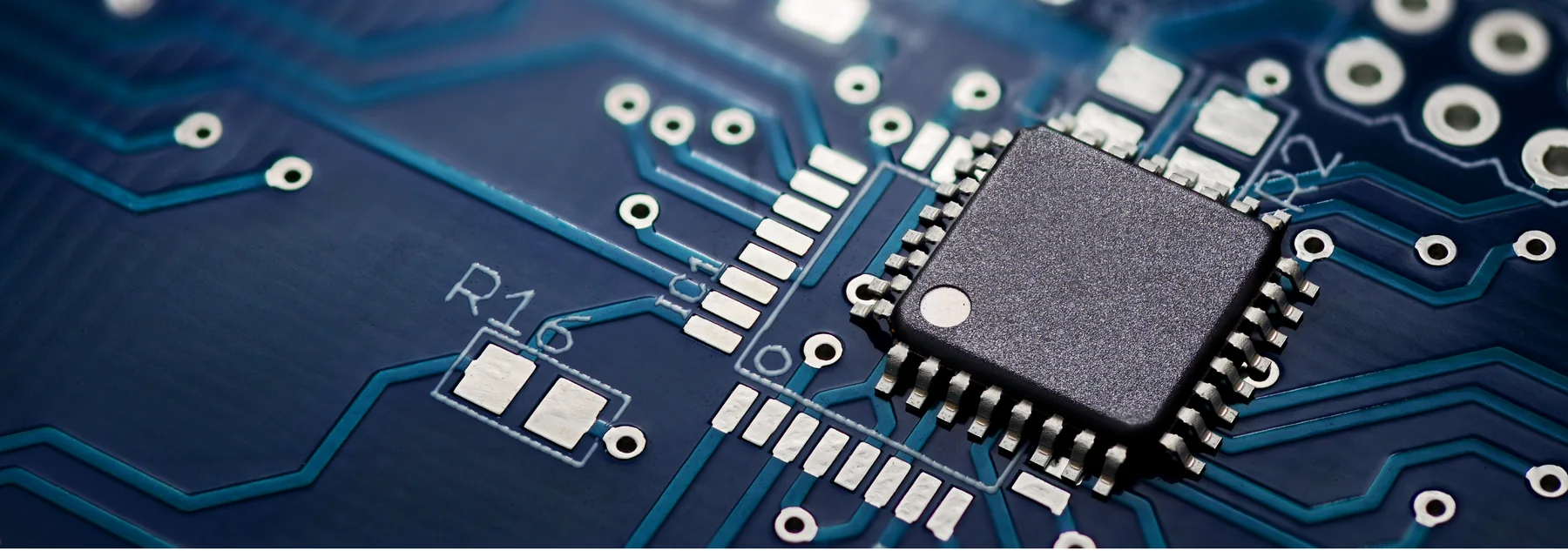 ISO 14644 · Cleanroom
Hinweis: Aktuell dienen die 3D-Modelle als Platzhalter. Sobald echte CAD-Daten vorliegen, werden sie durch die realen BEUTTER-Bauteile ersetzt.
We have all machining processes in-house and specialise in the high-depth manufacture of individual parts, components and complete assemblies for semiconductor and vacuum technology.
Vacuum and process components
- Vacuum-tight components for process and vacuum technology
- Defined sealing surfaces and tight tolerances
- Flanges, rings, housings and more
Plant & process components
- Precision components for wafer and chip manufacturing systems
- High requirements for dimensional and geometrical accuracy
- Made of titanium, stainless steel and aluminium
Purity & Surfaces
- Precision-machined sealing and functional surfaces up to Ra < 0.2 µm
- Multi-stage ultrasonic cleaning: aqueous
- Assembly and packaging in a cleanroom — ready for installation at the customer's site
Development & Assembly
- Complete development of system components
- Assembly of ready-to-install components from a single source
- Support from prototype construction to series production maturity – documented and traceable across the entire development process
„Where Purity and determine the process with micrometre precision."
For over 115 years, BEUTTER has been manufacturing components that the high-tech industry relies on — low-particle, process-reliable and manufactured for high cleanliness requirements in accordance with ISO 14644.
Haben Sie eine Zeichnung oder ein Bauteil?
Senden Sie uns Ihre Anforderungen — wir prüfen Machbarkeit, Werkstoff und Fertigung und melden uns mit einer kostenlosen Ersteinschätzung.
BEUTTER processes all machinable materials — specifically these for semiconductor technology:
For semiconductor and vacuum technology, alongside dimensional accuracy, cleanliness is of paramount importance. BEUTTER manufactures cleanroom-compatible components with defined, low-particle surfaces and complements the process with high-quality product cleaning for stringent cleanliness requirements.
The manufacturing process is fully documented and tested in the metrology laboratory using 100 % checks. In addition to manufacturing, we can, on request, undertake the complete development of system components as well as the assembly of ready-to-install sub-assemblies, all from a single source.
René Meier
72348 Rosenfeld
Your semiconductor technology project at BEUTTER.
From development through to the prototype and validated series — we support you with our comprehensive know-how and a free problem analysis by our experts.
Does BEUTTER manufacture cleanroom-compatible components for semiconductor technology?
Yes. BEUTTER manufactures precision components for semiconductor and vacuum technology and carries out high-quality product cleaning, ensuring cleanliness and low particle counts for high purity requirements in accordance with ISO 14644.
Which components does BEUTTER manufacture for the semiconductor industry?
BEUTTER manufactures vacuum and process components, parts for wafer and chip manufacturing equipment, and cleanroom-compatible assemblies, among other things—as individual parts, components, and ready-to-install assemblies.
What materials does BEUTTER process for semiconductor technology?
Among others, high-alloy and stainless steels, aluminium, technical ceramics and other special materials are used. In principle, BEUTTER processes all machinable materials.
How does BEUTTER ensure cleanliness and low particle levels?
The manufacturing process is documented and supplemented by high-quality product cleaning, which ensures cleanliness, low particle counts and defined surfaces for use in cleanroom and vacuum environments.
Have you got a drawing or a component?
Send us your requirements – we will check feasibility, material and production and get back to you with a free initial assessment.